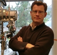
Olivier DOUHERET
Email: olivier.douheret@materianova.be
Phone: +32 (0) 65 55 49 67
Biosketch
Olivier Douhéret received a Civil Engineering degree in Physics from the Polytechnic National Institute of Grenoble (INPG), France in 2000. He then accomplished his doctoral studies in Physics at the Royal Institute of Technology (KTH) of Stockholm, Sweden and graduated his PhD in 2004.
His first postdoctoral position took place within the IMEC division of the Institute for Materials (IMO) in Diepenbeek, Belgium.
In 2007, he joined the Laboratory for Chemistry of Novel Materials (CMN) working as research scientist at Materia Nova R&D Centre.
From PhD studies to current activities, his field of work progressively expanded from conventional inorganic to organic semiconductors and from high resolution electrical characterization-based scanning probe microscopy methods towards fabrication and characterization of organic electronic structures such as electroluminescent and photovoltaic devices.
His past and current collaborations lie both within academic societies and industrial partnerships.
A few relevant publications of the past five years
V. Kozlov, Y. N. Luponosov, A. N. Solodukhin, B. Flament, O. Douhéret, P. Viville, D. Beljonne, R. Lazzaroni, J. Cornil, S. A. Ponomarenko and M. S. Pshenichnikov, “Simple donor-acceptor molecule with long exciton diffusion length for organic photovoltaics”, Organic electronics 53 (2018)
D. Moerman, N. Sebaihi, S. E. Kaviyil, Ph. Leclère, R. Lazzaroni and O. Douhéret, “Towards a unified description of the charge transport mechanisms in conductive atomic force microscopy studies of semiconducting polymers”, Nanoscale, 6, 10596-10603 (2014), DOI: 10.1039/C4NR02577F
O. Williams, O. Douhéret, M. Daenen, K. Haenen, E. Osawa and M. Takahashi, “Enhanced diamond nucleation on monodispersed nanocrystalline diamond“, Chemical Physics Letters, 445 (4-6), 255-258 (2007).
O. Douhéret, L. Lutsen, A. Swinnen, M. Breselge, K. Vandewal, L. Goris and J. Manca, “Nanoscale electrical characterisation of organic photovoltaic blends by conductive atomic force microscopy”, Appl. Phys. Lett. 89, 032107 (2006).
O. Douhéret, S. Bonsels and S. Anand, “Determination of spatial resolution in AFM-based electrical characterization techniques using quantum well structures” J. Vac. Sci. Technol.B. 23 (1), 61-65 (2005)

